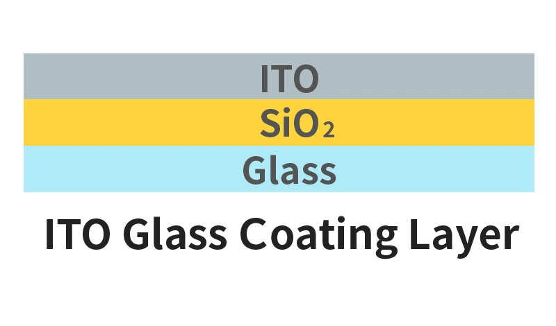
Hony Glass Technology's ITO (Indium Tin Oxide) transparent conductive glass—classified within the category of advanced optoelectronic glass—is manufactured using high-quality soda-lime, alkali-free glass or borosilicate substrates, onto which a uniform ITO thin film is deposited via a high-precision sputtering process.
The resulting product delivers stable electrical conductivity and excellent optical transmittance, supporting high-resolution displays, touch interfaces, and various optoelectronic components while providing a reliable conductive interface.In addition, EMI shielding functional layers can be incorporated according to product requirements. Through conductive mesh layers or multilayer optoelectronic stack designs, these solutions effectively reduce external electromagnetic interference (EMI) and enhance system noise immunity and signal stability. This makes the product particularly suitable for automotive displays, industrial control equipment, medical instruments, and high-precision measurement devices, where stringent electromagnetic resistance is required.
SiO₂ Barrier Layer
In LCD applications, SiO₂ functions as an ion-blocking layer that suppresses sodium ion migration toward the liquid-crystal region. In OLED and touch-panel applications, SiO₂ focuses on strengthening the adhesion between the ITO and the substrate, as well as providing dielectric isolation. It also enhances the film’s resistance to moisture, acids, bases, and chemicals, thereby reducing risks during subsequent manufacturing processes. Through precise control of film thickness and density, the optical-electronic module can maintain stable performance during long-term operation.


High-End Display Polished Substrates
For high-end display and OLED applications, Hony Glass Technology’s ITO glass is available with precision-polished substrates. By effectively reducing surface roughness (Ra) and improving overall flatness, the ITO thin film can be deposited with greater uniformity and stability. This characteristic not only enhances pixel alignment accuracy but also improves brightness and color uniformity across the panel. It plays an indispensable role in increasing yield for large-size and high-resolution displays.
Production Capability
LCD and Touch Panel (TP) Specifications
| Substrate Specification | |
|---|---|
| Substrate Size (mm) | 300 x 350 ~ 1300 x 1800 |
| Single-sided ITO Coating | ||
|---|---|---|
| Sheet Resistance Specification ( Ω / □ ) | Sheet Resistance Range ( Ω / □ ) | Transmittance ( % ) |
| SiO₂ | - | ≧ 92 |
| 5 | 4~6 | ≧ 78 |
| 7 | 5~7 | ≧ 78 |
| 10 | 7~10 | ≧ 80 |
| 15 | 9~15 | ≧ 84 |
| 25 | 10~25 | ≧ 80 |
| 30 | 15~30 | ≧ 80 |
| 50 | 25~50 | ≧ 82 |
| 60 | 30~60 | ≧ 84 |
| 80 | 50~80 | ≧ 86 |
| 100 | 70~100 | ≧ 88 |
| 125 | 80~125 | ≧ 88 |
| 250 | 200~300 | ≧ 90 |
| 400 | 320~480 | ≧ 90 |
| 500 | 400~600 | ≧ 90 |
| Double-sided ITO Coating | ||
|---|---|---|
| Sheet Resistance Specification ( Ω / □ ) | Sheet Resistance Range ( Ω / □ ) | Transmittance ( % ) |
| 5/G/500 | 4~6 | ≧ 77 |
| 400~600 | ||
| 120/G/120 | 100~140 | ≧ 87 |
| 100~140 | ||
| 150/G/400 | 100~200 | ≧ 86 |
| 320~480 | ||
OLED Specifications
| Substrate Specification | |
|---|---|
| Substrate Size (mm) | 300 x 350~370 x 470 |
| Substrate Thickness (mm) | 0.4~1.1 |
| Sheet Resistance Specification ( Ω / □ ) | Sheet Resistance Range ( Ω / □ ) | Transmittance ( % ) |
|---|---|---|
| 12 | ≦ 12 | ≧ 85 |
| 15 | ≦ 15 | ≧ 84 |
Applications
- LCD and OLED display panels
- Touch panels and human–machine interfaces (HMI)
- Automotive displays and smart home control panels
- BIPV building-integrated photovoltaics and transparent PV components
- Optical sensors and capacitive touch
- Flexible optoelectronic films and wearable devices
- Research, semiconductor, and industrial applications


